
VPItoolkit PDK LIGENTEC is a pluggable toolkit which extends VPIcomponentMaker Photonic Circuits by adding the support of the Silicon Nitride integrated photonics Process Design Kit (PDK) for the Multi-Project Wafer (MPW) runs offered by LIGENTEC.
It enables the rapid design of silicon nitride monolithically integrated photonic circuits based on the AN800 process for their subsequent fabrication at the LIGENTEC foundry.
VPItoolkit PDK LIGENTEC supports
IPKISS by Luceda Photonics and
PhoeniX OptoDesigner by Synopsys as layout design tools.
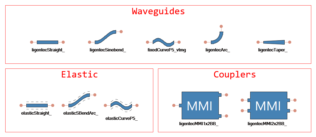
Overview of building blocks available in VPItoolkit PDK LIGENTEC
This demo illustrates design of an integrated optical buffer
circuit with custom building block (waveguide delay line) which has
a user-defined simulation model and layout.
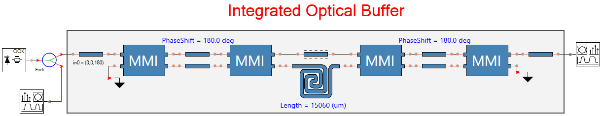
Simulation setup in VPIcomponentMaker Photonic Circuits
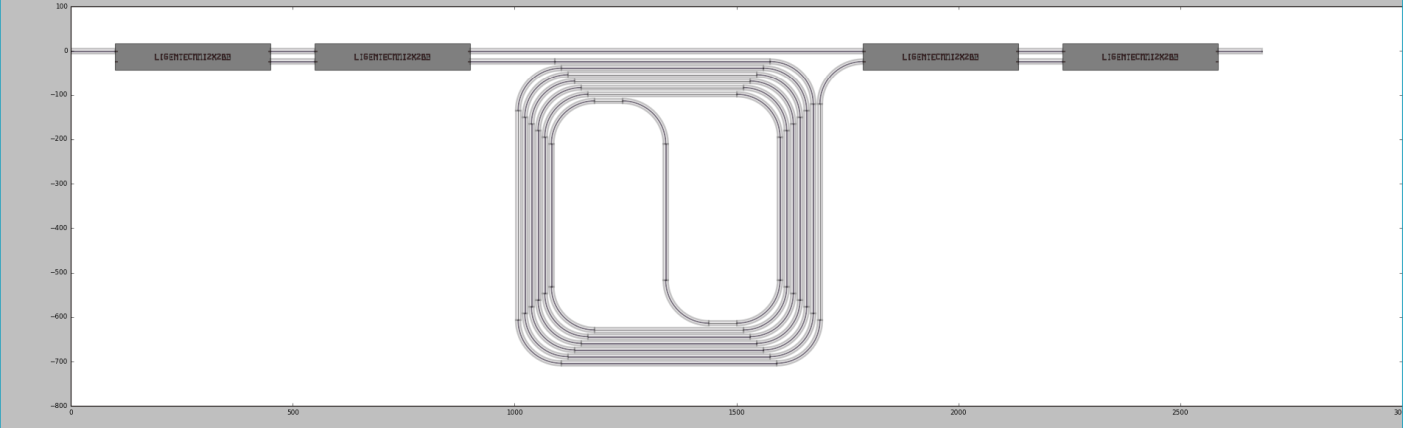
Automatically exported layout in IPKISS
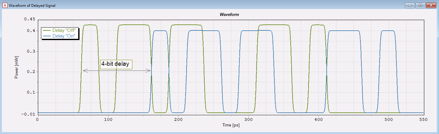
Simulation result for switched "Off" and switched "On" four-bit delay