

Photonic Design Environment (PDE)
In this tutorial, we'll explore the VPIphotonics Design Suite™ graphical user interface, or the Photonic Design Environment (PDE).
We will highlight the most common panels and dialogs to help you understand what you see when you first open the application.

1.6T ZR-based Coherent Superchannel Simulation
The simulation setup demonstrates the transmission of a 4x59.84 Gbaud superchannel. This solution can be considered as an upgrade of the 400G-ZR Optical Interconnect OIF
standard to a potential 1.6T ZR over a 75 GHz frequency grid. DP-16QAM is used as a modulation format and the transmission distance is set at 80 km. Pilot-aided carrier
frequency/phase recovery and data-aided TDE-MIMO is implemented at the receiver DSP for the 2nd tested channel. A Gardner clock recovery is used to compensate for a large
clock frequency mismatch of 500 MHz. Transmitter imperfections are considered and a BER pre-FEC is used as a performance metric. This simulation setup can be considered as
a baseline of hybrid WDM conventional QAM transmitters with pilot-aided QAM signals.

Visualize Photonics TLM Structure
One feature improvement introduced in VPIphotonics Design Suite™ v11.5 allows the user to visualize the Photonics TLM model and modify the
structure of the model through the visualization. This new automation feature allows for visual verification and simplifies what could be a complicated task. The Photonics TLM model
extends a well-established transmission-line laser model (TLLM) for designing multisection optoelectronic devices (lasers, SOAs, modulators, photodetectors) with support of MQW or
Bulk active media, flexible electrical contacts allocations, adjustable gain and absorption shapes, carrier dynamics and chirp models, spontaneous emission models, arbitrary profile
index and gain gratings (including nonreciprocal and sampled), reflective facets, Kerr, TPA, electro-refractive, electro-absorption, and many other effects.

Large-Scale Integrated Photonics Simulation – Interface Improvement
One user interface improvement introduced in VPIphotonics Design Suite™ v11.5 allows the user to extend their integrated photonics or optical
systems designs for large-scale integration. When schematics and designs reach the order of 100's or 1000's of components, it can be a daunting task to update each module
individually when a minor change is needed. We created additional automation tools to make these tasks a breeze. The Object Browser allows you to navigate all of the modules used in a
schematic. The new functionality gives you the ability to select and change parameters in multiple modules all at once. It also offers flexibility in what modules are selected, and we
provide a macros allowing you to automate the creation of a switch matrix which can simplify the design of optical circuit switches and other programmable photonics applications.

Fast Setup of Coherent WDM System Simulations
One of the new features in VPIphotonics Design Suite™ v11.5 is a macro allowing you to setup a Coherent WDM System simulation in just minutes.
The new macro labeled 'Synthesize QAM WDM Link' is now available for use. It supports both coherent wavelength-division multiplexing (WDM) and single-channel configurations.
Dual polarization multi-level quadrature amplitude modulation (DP-mQAM) channels are considered. A flexible digital signal processing (DSP) unit is integrated and the macro provides
indications of parameter thresholds to enable fast optimization.

Modeling Multicore Fiber Transmission
One of the updates in VPIphotonics Design Suite™ v11.5 is the ability to model multicore fiber transmissions with the new FiberMCF_MM Module.
The FiberMCF_MM module is designed to simulate signal propagation in weakly coupled single-mode multicore fibers (MCFs). These advanced fibers enhance the capacity of optical links,
making them ideal for both short-reach and long-haul transmission systems utilizing Space Division Multiplexing (SDM) technology. The module accurately models various detrimental effects,
including loss, chromatic dispersion, polarization mode dispersion, and Kerr nonlinearity. It replicates the effects in parameters in both the physical and numerical intracore categories,
such as crosstalk and fiber skew, and intercore effects, such as distributed power coupling, in standard FiberMM models. Explore how the various fiber parameters and deployment conditions
affect the characteristics of optical links with the FiberMCF_MM module.

Make parameter expression creation a breeze
Denis Kruchkov, the development leader at VPIphotonics, explains how to use the Parameter Watch functionality of
VPIphotonics Design Suite™to simplify the task of validating parameter values of complex expressions.
The feature is useful for debugging and optimizing designs.

How to design an
FMCW LiDAR system using
VPItransmissionMaker Optical Systems
(Part 1)
Dr. Nebras Deb, an optical systems application specialist at VPIphotonics, explains how to design an FMCW LiDAR system using
VPItransmissionMaker™ Optical Systems. Both the target distance and velocity are extracted using
spectral analysis of the received signal.

How to predict and simulate
the design constraints of an
FMCW LiDAR system
(Part 2)
Eugene Sokolov, a principal application engineer at VPIphotonics, explains how to predict and simulate the design constraints
of a FMCW LiDAR system using VPIcomponentMaker™ Photonic Circuits. We discussed the impact of the
residual nonlinearity of the laser and how digital predistortion could help to mitigate this effect.

Automated approach of optimization
to traffic grooming in DWDM Networks
Do you need to optimize the number of wavelength/optical channels required to carry client connectivity services over the whole DWDM network according to engineering rules to meet system requirements?
Dmitry Khomchenko, the product manager of VPIlinkDesigner™ and VPIlinkConfigurator™ at VPIphotonics™, demonstrates the automated
approach to traffic grooming in VPIlinkConfigurator.

How to Simulate
Multisection Semiconductor Lasers
with VPI Design Suite
As part of VPIphotonics Design Suite™, VPIcomponentMaker™ Photonic Circuits can help you model some advanced multisection semiconductor devices.
In this video, we demonstrate how to simulate a three-section tunable laser diode using our software. We first describe the fundamentals of the Photonics TLM module. Then, we show how to create
such a structure using VPIphotonics Design Suite. And finally, we explain how to do the characterization of the simulated device with the help of the Characterize Laser macro.

Trilogy PAM-4 Transmitter – Part 1:
Schematic creation, parameter editing, sweeps and optimization
In the first episode of our video trilogy, we demonstrate how to use VPIcomponentMaker™ Photonic Circuits as part of
VPIphotonics Design Suite™ to simulate a PAM-4 transmitter. We cover the main software functionality and guide you through
a design of a simple Mach-Zehnder modulator. Moreover, we create schematic parameters, perform a parameter sweep, and optimize the design.

Trilogy PAM-4 Transmitter – Part 2:
Hierarchical structures with galaxies, parameter expressions and scripts
In the second episode, we create a dual-parallel Mach–Zehnder modulator to serve as a basis for a final design of the PAM-4 transmitter,
using VPIcomponentMaker™ Photonic Circuits as part of VPIphotonics Design Suite™.
We demonstrate how to make a hierarchical design with the help of the regular galaxies, add galaxy parameters, and define them using mathematical and
Python expressions as well as initialization scripts in parameter settings.

Trilogy PAM-4 Transmitter – Part 3:
Simulation domains, multiple runs and visualization
In the third episode, we finalize our design of the PAM-4 transmitter, using VPIcomponentMaker™ Photonic Circuits as part of
VPIphotonics Design Suite™. We discuss time domain and hybrid time-and-frequency domain simulations, resolve deadlock issues,
carry out simulations with multiple runs, and visualize an eye diagram of our transmitter.

How to Optimize Add/Drop Equipment Configuration
Need to configure your add/drop equipment and allocate wavelengths for a new network or a network upgrade? Dmitry Khomchenko, the product manager of VPIlinkDesigner™ and
VPIlinkConfigurator™ at VPIphotonics™, shares tips on how to delegate all the time-consuming tasks (like reusing previous equipment and minimizing link loading)
to the design automation tool available in VPIlinkConfigurator.

Electrical-Optical-Electrical (EOE) System
Simulation with PathWave ADS
Keysight Technologies and VPIphotonics have partnered to create the industry first electrical-optical-electronic (EOE) solution to test an end-to-end link. This video will cover what the solution is and how it works through a quick demo.

Highlights of talk given at the EPIC World
Industrial Quantum Photonic Technology
Summit in Barcelona in June 2019
Dr. Igor Koltchanov, Director Technology, is presenting the highlights of his talk given at the EPIC World Industrial
Quantum Photonics Technology Summit 2019. The video explains how a classical simulation framework can be applied for modeling
quantum communications with focus on weak-coherent CV QKD protocols.

Nonlinear Noise Cancellation Using Phase-Conjugated Twin Waves:
How to combat Kerr induced distortions
Ksenia Goroshko, an optical engineer at VPIphotonics, explains how to mitigate fiber nonlinearities
using the twin waves technique. She demonstrates the power of this method by running an exemplary
schematic in the simulation software VPIphotonics Design Suite™
for different parameter settings.

Laboratory experiments made easy:
How to validate simulation results in your lab and to make the best of automated simulation
In this video, we show how to use VPIlabExpert™ as part of our
VPIphotonics Design Suite™ to transmit a discrete multitone
(DMT, real-valued OFDM) signal through a real link accessing lab equipment like a Tektronix 70000
series AWG and a Tektronix DPO70000SX oscilloscope here. We further demonstrate how you can perform
bit-and-power loading by controlling schematic runs with a Python script to increase the system
capacity while ensuring a minimum performance metric for all the subcarriers.

Next-generation high-speed transceivers:
Solving the dilemma of more capacity and less cost
VPItransmissionMaker™ Optical Systems accelerates the design of new photonic systems and
subsystems for short-range, access, metro and long-haul optical transmission systems and allows technology upgrade and component
substitution strategies to be developed for existing fiber plants.

Versatility in modeling and optimization of PICs
VPIcomponentMaker™Photonic Circuits is a simulation and design environment for modeling
photonic integrated circuits (PICs). It provides advanced device libraries integrated with a scalable time-and-frequency-domain
simulation framework enabling fast and accurate modeling of large-scale PICs with a mix of photonic, electrical and optoelectronic
devices.

Connectivity for design flow and manufacturing automation
See the video below for more details about how to export a circuit designed with VPItoolkit™ PDK HHI into PhoeniX OptoDesigner.

Modeling and Optimizing PICs
for Datacenter Interconnects
Datacenter traffic is growing exponentially, driven by demanding applications like AI/ML Training, Cloud Computing, and Video Streaming.
Photonic integrated circuits (PICs) have become an enabling technology in the rapid expansion of datacenter connectivity due to their lower cost,
lower power consumption, small footprint, and high-speed performance.
One of the main challenges of utilizing PICs for datacenter applications is the design complexity associated with their integration into a
fiber-optic communication system. Specifically, impairments stemming from the PIC may not be recognized until its performance validation in the
application of interest. As a result, optimizing the PIC parameters in the context of the entire system is crucial to making informed decisions
about technology choices and design alternatives.
In this tutorial, we explore the photonic design process at both the circuit and the system level. Join us to learn how to automate the design
of PICs and simulate high-speed optical transmission systems using VPIphotonics Design Suite™.

Simulating Datacom/Telecom Scenarios in Compliance with 800G and 1.6T Standards
In this tutorial, you will gain insights in conceptualizing and analyzing optical transmission systems for short-reach applications.
We will demonstrate how to utilize professional simulation software while adhering to recommendations from standardization committees and
multi-source agreements (MSAs). We will explore the design and performance of 800G-FR4 systems, incorporating forward error correction (FEC)
with intensity modulation and direct-detection (IMDD). Additionally, we will examine the transmission characteristics considering the
400GBASE SR4.2 standard which utilize multimode vertical cavity surface emitting lasers (VCSELs) and multimode fibers. Lastly, you will
acquire knowledge on designing and evaluating both 400G and 1.6T ZR transmission by leveraging advanced digital signal processing (DSP)
techniques for coherent technology. The tutorial will demonstrate how to efficiently automate the design and analysis processes for new
standards recommendations. You will also gain insights into examining the impact of performance-limiting effects.

Simulation of Classical & Quantum Communications over FSO Satellite Links
Free space optical (FSO) communication technology based on the optical signal transmission through a free-space channel has gained significant interest in recent years. FSO satellite links have the potential to establish a global
all-optical communication network that could cope with the increasing demands for high data rates and communication capacity. Moreover, satellite-based quantum key distribution (QKD) could provide secure and private communication between
distant users. VPIphotonics Design Suite offers advanced means for simulation of both classical and quantum optical communication systems for terrestrial and satellite FSO links. In this webinar, we focus on modeling aspects of FSO signal
transmission in ground-to-satellite, satellite-to-ground, and intersatellite links. We will also work through a few live demos of application examples and investigate the FSO system performance in presence of such adverse effects as
atmospheric scintillation, attenuation, beam diffraction, and pointing errors. In addition, we discuss the satellite-based quantum key distribution and demonstrate how the performance of the QKD link depends on a satellite's position and
other link parameters.

Optical Link Design Automation from Access to Core Networks
Recent growth in the deployment of xHaul networks including metro and core networks triggers the application of very different technologies to support the increase in link distances and traffic. Critical network design constraints
include dense wavelength division multiplexing (D)WDM of channels operating at different data rates, and the deployment of optical amplifiers and dispersion compensation modules (DCMs) to meet power and dispersion budget requirements.
Cost-optimized planning of such networks is a challenging task considering the diverse equipment constraints. In this webinar we demonstrate an automated network design that efficiently addresses the challenges and requirements for
various types of networks.

New Interoperable Software Platform for the Design of Photonic Devices
As a leader in photonic design automation for components, systems and networks, we will introduce a new interoperable software platform for the design of photonic devices, empowering researchers to explore new designs for photonic
integrated circuit (PIC) passive components and optical fibers. This new platform streamlines the migration of device-level simulation data into a circuit-level simulator for the design and optimization of PICs. We will give an overview
of the new platform and describe how it fits into our current ecosystem of photonic design and simulation tools.

Automated PIC Modelling:
A Photonic Neural Network Use Case
As the complexity of Photonic Integrated Circuits (PICs) continues to grow, testing environments become more complicated. In this webinar, we will present several simulation testbenches prepared for visualizing typical
measurement characteristics. The examples we will discuss include methods for group index verification, simulation of passive circuit transfer functions, characterization of SOAs, and evaluating the transfer characteristic of
an Activation Unit for a Photonic Neural Network. These examples will all be demonstrated live using the photonic design automation (PDA) software VPIcomponentMaker Photonic Circuits.

PIC Magazine talks with Chris Maloney, Director of Business Development at VPIphotonics

Paving the Way for InP Photonic Integrated Circuits from Concept to Tape-out
Streamlining the design process, shortening the development cycle, and reducing the transition to manufacturing remain some of the most demanding requirements for photonic integrated circuit (PIC) designers.
During this webinar, Infinera and VPIphotonics will present a design and fabrication workflow for InP PICs developed to address these needs. The workflow is based on the Infinera Process Design Kit (PDK), which
includes devices optimized to ensure the best performance and yield within Infinera's InP foundry. VPIphotonics and Infinera collaborated to develop compact models for these PDK building blocks to allow for rapid
prototyping of application-specific PICs. Join our webinar to learn how to start your PIC design with a graphical circuit representation and system simulation in VPIphotonics' software environment and smoothly
proceed with physical layout implementation, verification, and fabrication by Infinera's InP foundry.
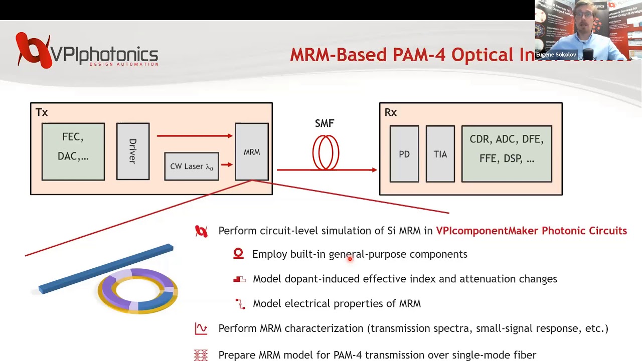
Migrating a PIC Simulation to a System Design: Silicon-Photonic Modulator in a PAM-4 Link
Dr. Jim Farina, Chris Maloney and Eugene Sokolov show how to migrate a PIC simulation to a system design.
Modeling and
simulation at both the circuit- and system-levels are critical in the design process for optical communication, quantum key
distribution, and sensing applications. Seamless migration between these two levels of abstraction will be demonstrated in
VPIphotonics Design Suite. This webinar focuses on an optical communication application example by modeling a silicon-photonic
modulator at the circuit-level and implementing it for simulation at the system-level in a PAM-4 link.

Design Optimization and Sensitivity Analysis of Photonic Integrated Circuits using Physical and Circuit-Level Simulations
The use of highly-integrated photonic circuits (PICs) is on the rise, and this trend is expected to accelerate in the future.
The design of these complex circuits involves multiple steps, starting at the component level and continuing up to the circuit level.
Due to this hierarchical structure, small variations at the component level resulting from fabrication tolerances can have a significant
influence on the overall circuit performance.
This eSeminar focuses on two software packages, which combine advanced simulation of passive photonic, active optoelectronic and hybrid
photonic integrated circuits and systems with highly accurate full-wave 3D photonic and multiphysics simulation.
We will demonstrate how using VPIphotonics Design Suite and CST Studio Suite together enables engineers designing PICs to automate
combined circuit level and full wave simulation. This allows the study of the effect of small variations in the components on the
overall circuit, meaning that the engineer can increase yield and reliability by making the circuit resilient to such effects.

Talk at PIC International Online Summit, 19th May 2020
Versatile design tools for integrated photonics and optoelectronics need to support a diversity of technologies addressing
very different types of applications. We discuss stringent requirements imposed on them: PICs of increasing size and complexity
require circuit-level simulators supporting hierarchical topologies and automation of circuit design. PIC performance testing in
target application scenarios requires the seamless integration of circuit- and system-level design tools. An automated design of
EO/OE interconnect solutions, especially of importance for telecom and datacom, requires dynamic communication and seamless data
transfer between electronic and photonic design tools.

Talk at ONDM 2020 - 24th International conference on Optical Network Design and Modelling
D.Khomchenko, A. Richter, and J. Farina (@VPIphotonics) demonstrate an algorithmic approach that efficiently addresses
the link loss and dispersion compensation and equipment allocation problem for xhaul networks. It accounts for future channel
loading, optical channel path parameters, signal rate, equipment parameters, and constraints arising from the insertion points
of amplifiers and DCMs. The authors demonstrate the convenient operation of their method by designing an exemplary fronthaul
network system.

Machine Learning Framework for Designing and Implementing
Deep Neural Networks
VPItoolkit™ ML Framework is a versatile add-on to any of the simulation tools of
VPIphotonics Design Suite™, enabling the implementation and design of deep neural networks
(DNN) for various applications, such as equalization and nonlinearity mitigation for optical systems, device characterization,
evaluation and inverse design of photonic devices.

Automating the Design of PIC-Based LiDAR Systems
Originally developed for military use in the 1960's, Light Detection and Ranging (LiDAR) technologies are now being used for medical,
agricultural, environmental, civil engineering, space exploration and automotive applications. The adoption of LiDAR for autonomous driving is
likely to be the first widespread commercial use for LiDAR. Coherent LiDAR systems measure both the phase and amplitude of the return signal,
allowing for the measurement of both the distance and velocity of an object simultaneously, making it an ideal candidate for autonomous driving
applications. In gaining such widespread adoption, size, weight and cost of such systems must be significantly decreased. One way to achieve
such benefits is to leverage the advantages of integrated photonics.
Provided the great variety of the LiDAR design approaches and technologies, the software tools need to be flexible in simulating them, supporting multiple existing solutions, and interfacing between different third-party tools. At the same time, the need for high volume manufacturing and growing complexity of photonics integrated circuits (PIC) both require specific design and simulation solutions for PIC-based devices.
In this industry tutorial, you will learn how to streamline the design process using VPIphotonics Design Suite™ considering a Frequency Modulated Continuous Wave (FMCW) LiDAR system. We will discuss how to predict and simulate the design constraints of such systems. Particularly, we will discuss the impact of the residual nonlinearity of the integrated tunable laser and how digital predistortion could help to mitigate this effect.
Transmission aware Multiple Lightpath Reconfiguration in Flexgrid Optical Networks
We present an algorithmic approach that offers an efficient way of multiple lightpaths reconfiguration, either for increased traffic requests, or lightpath restoration. It permits the building of a feasible optical network design considering the available spectrum, traffic
demand characteristics, network topology, equipment configurations, and engineering constraints. We show the employment of methods for calculating and provisioning multiple lightpaths. Our approach is flexible enough to accommodate optical network topologies of different types and sizes. The result
is a lightpath configuration that is optimized for spectrum utilization and GSNR degradation.

A simulation environment for
QKD systems and co-existing classical channels
Recently VPIphotonics developed a new simulation tool, VPItoolkit QKD. When used together with VPItransmissionMaker Optical Systems, a simulation environment for classical transmission systems, they represent a powerful R&D environment
for the development of QKD systems based on weak-coherent prepare-and-measure protocols, including co-existence scenarios with classical channels. The design environment can serve as a test bed for the development and evaluation of various
implementation options of QKD systems and sub-systems, such as pulse shaping, signal recovery and filtering, and others.

Transmission-Aware Bandwidth Variable Transceiver Allocation in DWDM Optical Networks
Talk presented by Dmitry Khomchenko on 1 July 2021 at ONDM 2021.
This presentation addresses the transmission-aware transceiver allocation problem of flexible optical networks for a multi-period planning.
The proposed approach aims at assigning the best configuration of bandwidth variable transceivers (BV-TRX) considering the amplifier noise
and nonlinear channel interferences using the incoherent Extended Gaussian Noise (EGN) model. The proposed solution improves the network
throughput and spectrum utilization in the early planning periods and allocates lower number of BV-TRXs in later periods in comparison to
algorithms presented recently. A heuristic approach to regenerator placement has also been applied achieving up to 25% transceiver and
50% spectrum utilization savings in comparison to configurations without regenerators.

Talk at AngelTech Virtual Live III, 12th April 2021
PIC fabrication tolerances are inevitable and strongly degrade device yield, unless their impact on overall performance characteristics
is considered during the design process. We present a general-purpose schematic-driven design framework that provides easy access to statistical
performance techniques. By introducing a novel method that allows for the identification of critical light paths and applying automated phase
compensation inside the models, the analysis of fabrication tolerances on-wafer and between wafers is significantly simplified. We demonstrate
its application in several PIC designs including complex photonics-based neural networks.

A glimpse into the crystal ball of photonic design automation
Talk at PHOTONICS+, 18 February 2021
In this forward looking talk given during the Photonics+ Virtual Conference and Exhibition, we discuss the future of photonic design automation and applications being enabled by design software. VPIphotonics Design Suite is an
ever-evolving suite of software that is leading the industry as a result of collaborative industry and research partnerships as discussed in this presentation. In particular we discuss advancements in electrical/optical co-design
for intra-datacenter links, quantum key-distribution, PIC foundry PDKs, and application specific PICs such as: optical coherence tomography, 2D beam steering for LIDAR, and plasmonic neural networks.

Talk at AngelTech Virtual Live II, 2nd November 2020
We present an environment supporting top-level co-design of complete Electrical-Optical-Electrical (E-O-E) interconnect solutions and co-simulation of integrated electrical and optical components and sub-circuits.
This is enabled by dynamic communication and seamless data transfer between electronic and photonic design tools. Quick behavioral models (based on IBIS-AMI) of complex electrical circuits are combined with detailed
optical and electro-optical models for lasers, optical modulators, fibers, etc. that operate at different abstraction levels. The detailed modeling of purely electrical components (e.g. drivers, TIAs, equivalent circuits
of EO / OE components) into this hierarchical design flow is enabled by integrating a SPICE simulation engine.

Advanced DSP and Coding for Next Generation Coherent Optical Systems
Next generation coherent optical systems are expected to deliver high data rates to meet the increase of traffic demands
driven by the emergence of high-bandwidth applications, such as Internet of Things, 4K video streaming, and online gaming.
Different technologies have been proposed and investigated for next generation 400G, 800G, and 1.6T systems. In this webinar,
we review the most promising techniques including, advanced modulation formats and coding, fiber nonlinearity mitigation, and
space division multiplexing. All demonstrations will be performed in VPIphotonics Design Suite.

Talk from Dr. Andre Richter at PIC International Conference on 10th April 2018 in Brussels
Efficient and convenient solutions for electronic photonic design automation (EPDA) present fundamental prerequisites
for the fast and innovative development of next-generation integrated photonic and optoelectronic circuits. In the talk
held at PIC International 2018 in Brussels (Belgium) we demonstrated how a layout-aware
schematic-driven methodology enables the rapid prototyping of new design concepts, including parameter optimization of
photonic and electronic parts, analysis of manufacturing tolerances, and comparison of technology and integration
alternatives to highlight progress in this area.

Interview with Jim Farina at NGON US 2016
The NGON US team interviewed Jim Farina, director of technical services at VPIphotonics™ –
he spoke about VPIphotonics, the key challenges the company is currently facing, his opinion on the state of the North American market,
and also the importance of events like Next Generation Optical Networking for the industry as a whole.

Talk from Dr. Andre Richter at ECIO in May 2016 in Warsaw
Fast and accurate circuit-level modeling:
A new scalable simulation approach